BYU-led research team develops world's most power-efficient ADC microchip
The ADC developed by BYU researchers consumes only 21 milli-Watts of power at 10GHz for ultra-wideband wireless communications as opposed to current ADCs that consume hundreds of milli-Watts or even Watts of power at comparable speeds.
- Country:
- United States
Researchers led by a team at the Brigham Young University (BYU) claim to have created the world's most power-efficient high-speed analog-to-digital converter (ADC) microchip. As the name suggests, an ADC is an electronic system that converts an analog signal, such as radio waves or a sound picked up by a microphone into a digital signal.
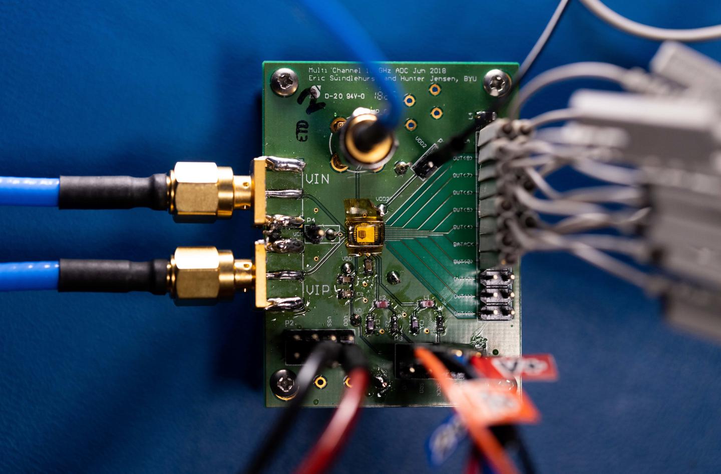
BYU professor Wood Chiang, Ph.D. student Eric Swindlehurst and their team developed the ADC with the highest power efficiency currently available globally. The team included collaborators from Taiwan's National Yang Ming Chiao Tung University and the University of California, Los Angeles.
The ADC developed by BYU researchers consumes only 21 milli-Watts of power at 10GHz for ultra-wideband wireless communications as opposed to current ADCs that consume hundreds of milli-Watts or even Watts of power at comparable speeds.
The researchers reduced the loading from a digital-to-analog converter (DAC) by scaling both the capacitor parallel plate area and spacing, making the converter faster and more efficient. They also grouped together unit capacitors that are part of the same bit in the DAC rather than having them be interleaved throughout. This helped lowered the bottom-plate parasitic capacitance by three times, significantly lowering power consumption while increasing speed.
Next, they used an improved bootstrapped switch by making it dual-path where each path can be independently optimized, resulting in increased speed while eliminating the need for additional hardware as it involves splitting existing devices and making route changes in the circuit.
Chiang said that the technology will result in a lot of conveniences for consumers. For instance, WiFi will get better with faster upload and download speeds and people will be able to watch 4K or even 8K with little to no lag while maintaining battery life.
The project was sponsored by the Ministry of Science in Taiwan and a consortium of technology companies. Details of the project are published in the IEEE Journal of Solid-State Circuit with Swindlehurst serving as the principal author.


