Samsung's cutting-edge 3D TSV technology can stack up to 12 DRAM chips
Featuring a shorter data transmission time as compared to the existing wire bonding technology, the latest advancement offers significantly faster speed and lower power consumption.
- Country:
- Korea Rep
South Korean technology giant Samsung has developed the industry’s first 12-layer 3D-TSV (Through Silicon Via) chip packaging technology that is considered as one of the most challenging packaging technologies for mass production of high-performance chips.
The cutting-edge 12-layer 3D TSV technology needs pinpoint accuracy to vertically interconnect 12 DRAM chips through a three-dimensional configuration of more than 60,000 TSV holes, each having a width one-twentieth of the thickness of a human hair.
According to Samsung, the 12-layer DRAM package maintains the same thickness as current 8-layer High Bandwidth Memory-2 (HBM2) products i.e. 720 micrometers and this will help customers release next-generation products with higher performance capacity without having the need to change their system configuration designs.
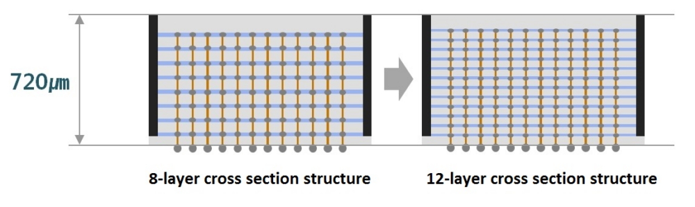 Image Credit: Samsung
Featuring a shorter data transmission time as compared to the existing wire bonding technology, the latest advancement offers significantly faster speed and lower power consumption.
“Packaging technology that secures all of the intricacies of ultra-performance memory is becoming tremendously important, with the wide variety of new-age applications, such as artificial intelligence (AI) and High Power Computing (HPC),” said Hong-Joo Baek, executive vice president of TSP (Test & System Package) at Samsung.
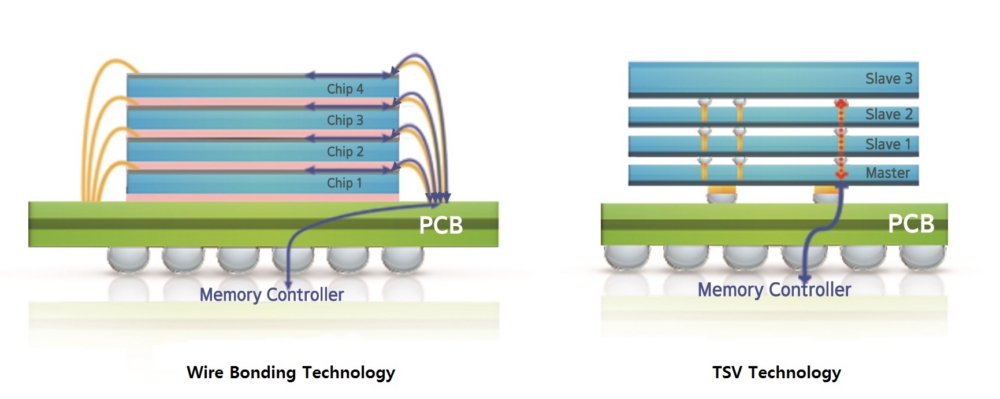 Image Credit: Samsung
With the increase in the number of stacked layers, from eight to 12, the advanced semiconductor tech giant will able to mass-produce 24GB High Bandwidth Memory solutions, which will provide three times the capacity of the currently existing 8GB HBM chips and offer the highest DRAM performance for applications that are data-intensive and extremely high-speed, the company said in a press release.
- READ MORE ON:
- Samsung
- 12-Layer 3D-TSV
- DRAM chips
- 8GB HBM chips
ALSO READ
Samsung launches Galaxy M55 5G and Galaxy M15 5G in India
Samsung to get $6-7 billion in chip subsidy next week for Texas expansion, sources say
Samsung Elec shares priced for $326 mln block sale, sources say
Samsung Elec shares priced at 84,100 won each in $326 mln block sale, sources say
US to award Samsung up to $6.6 billion chip subsidy for Texas expansion, sources say


