India Achieves Breakthrough in 3nm Chip Design with New Renesas Centres
While addressing the gathering at the launch event, Shri Vaishnaw emphasized the strategic importance of this development.
- Country:
- India
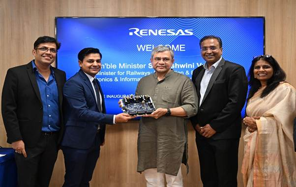
In a major leap for India's semiconductor ambitions, Union Minister for Electronics & Information Technology, Railways, and Information & Broadcasting, Shri Ashwini Vaishnaw, today inaugurated two state-of-the-art chip design facilities of Renesas Electronics India Private Limited, located in Noida, Uttar Pradesh, and Bengaluru, Karnataka. These new facilities are set to become pivotal components of India’s growing semiconductor ecosystem, with one of the design centers reportedly pioneering India’s first-ever 3 nanometer (3nm) chip design capabilities.
India’s Entry into the Global 3nm League
While addressing the gathering at the launch event, Shri Vaishnaw emphasized the strategic importance of this development. “Designing at 3nm is truly next-generation. We’ve achieved success in 7nm and 5nm designs in the past, but entering the 3nm space places India among the select few nations capable of this cutting-edge technology,” he stated.
The move signals India's emergence as a serious player in global semiconductor innovation—a field traditionally dominated by countries like the United States, South Korea, Taiwan, and Japan. The 3nm process node represents a major technological advancement, offering significant improvements in power efficiency and performance for computing devices ranging from smartphones to supercomputers.
A Holistic Strategy for Semiconductor Leadership
Minister Vaishnaw also elaborated on India’s comprehensive strategy for semiconductor growth, encompassing the entire value chain—from design and fabrication to ATMP (Assembly, Testing, Marking, and Packaging), along with indigenous development of equipment, chemicals, and gases required for chip manufacturing.
“Our ecosystem is maturing. We are seeing growing interest and confidence from global players, evident at international platforms such as Davos. Companies like Applied Materials and Lam Research have already begun investing in India’s semiconductor landscape,” the Minister noted.
He stressed that the inauguration of these design centres in Noida and Bengaluru reflects the government’s focus on distributing semiconductor capabilities across India, rather than limiting them to a few urban hubs. “With every new center, we are taking a step closer to building a pan-India semiconductor ecosystem,” he said.
Talent Development through Education and Training
A key aspect of India's semiconductor mission lies in its investment in human capital. To this end, the Minister unveiled a new semiconductor learning kit aimed at strengthening the practical hardware skills of engineering students. These kits are designed to complement the EDA (Electronic Design Automation) software tools already distributed to more than 270 academic institutions through the India Semiconductor Mission (ISM).
“This integration of hardware and software training is not just infrastructure building—it’s talent nurturing. We are creating a generation of engineers who are job-ready and globally competitive,” said Shri Vaishnaw.
He lauded the contributions of CDAC (Centre for Development of Advanced Computing) and the ISM team for their robust implementation of training programs and infrastructure development, which are crucial to sustaining the momentum of India’s chipmaking journey.
Industry and International Partnerships
During the ceremony, Shri Hidetoshi Shibata, CEO & MD of Renesas Electronics Corporation, highlighted India’s rising importance in the company’s global strategy. “India is now a strategic cornerstone for Renesas. Our teams here contribute significantly to embedded systems, software development, and system-level innovations,” he said.
Shibata reiterated Renesas’ commitment to developing end-to-end semiconductor capabilities in India—from architecture to testing. The company also intends to actively support over 250 academic institutions and numerous startups, in alignment with Government-backed programs such as PLI (Production Linked Incentive) and ISM.
He added that India’s vast talent pool, combined with the strategic Indo-Japanese cooperation, holds the potential to “reinvent the global semiconductor lifecycle.”
Aligned with Aatmanirbhar Bharat Vision
Shri Vaishnaw expressed his gratitude to Prime Minister Shri Narendra Modi, under whose leadership the semiconductor sector has been declared a strategic priority. This move aligns with the broader Aatmanirbhar Bharat (Self-Reliant India) mission.
“In just three years, India’s semiconductor industry has gone from being nascent to becoming a recognized emerging hub. This trajectory shows promise for long-term, sustainable growth,” the Minister asserted.
As digital infrastructure grows across sectors like smartphones, laptops, defense, medical equipment, and automobiles, the demand for semiconductors is set to rise exponentially. “This is the right time to accelerate our efforts. The future is digital, and semiconductors are at the heart of it,” he concluded.
India’s Silicon Leap
The launch of these cutting-edge facilities by Renesas is a landmark moment that affirms India’s ambition to become a global hub for semiconductor innovation. With a balanced focus on technological advancement, educational reform, and strategic global collaboration, India is now entering an era where it can define the future of chip design and electronics manufacturing.


